Generating Bitstream in Vivado
Step 1
For Linux User:
Create a new folder, and move the zip file to this folder, run the shell commond:
mkdir adderProject
cd adderProject
mkdir IPs
cd IPs
mv ../../vector_add/vector_add/solution1/impl/export.zip ./
unzip export.zip
For Windows User:
Create a new folder (e.g., C:\Users\twei2\workspace\course\adderProject)
Crete a folder and call it IPs
upzip the zip file in the IPs folder
Step 2
For Linux User:
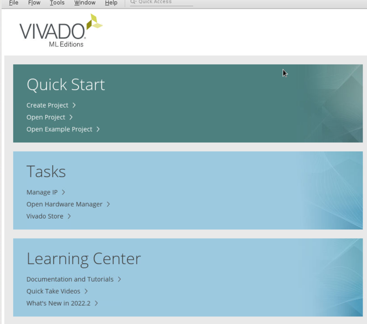
Invoke Vivado GUI, run the shell commond:
vivado
For Windows User:
Launch Vivado
Step 3
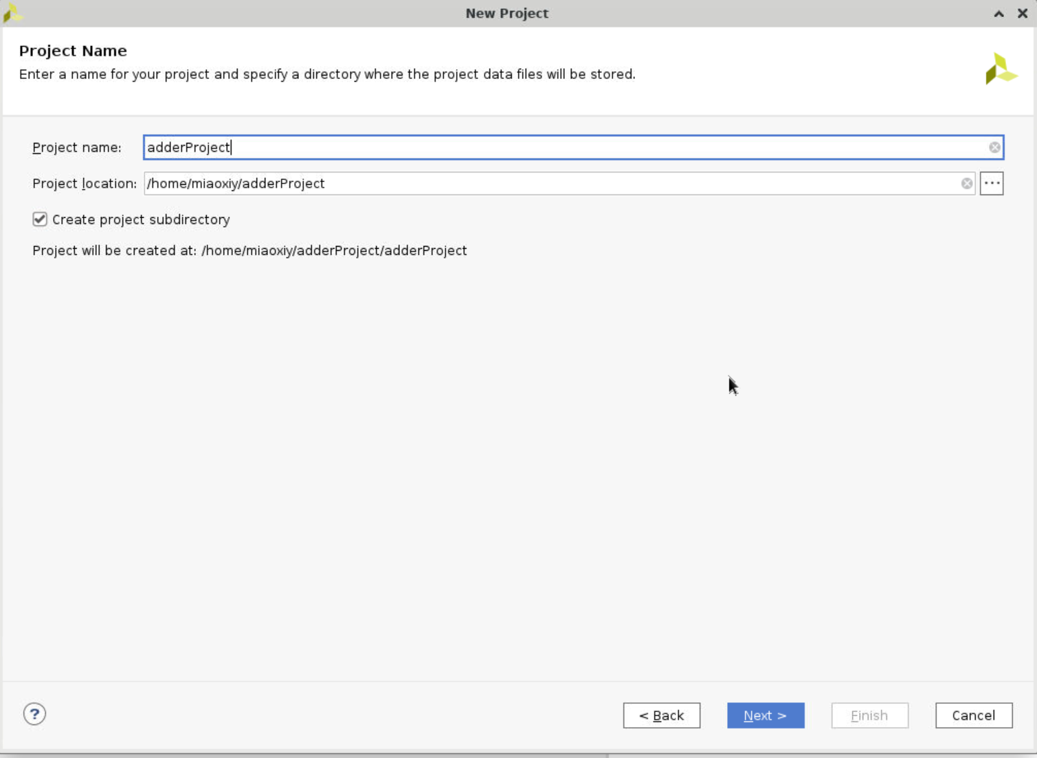
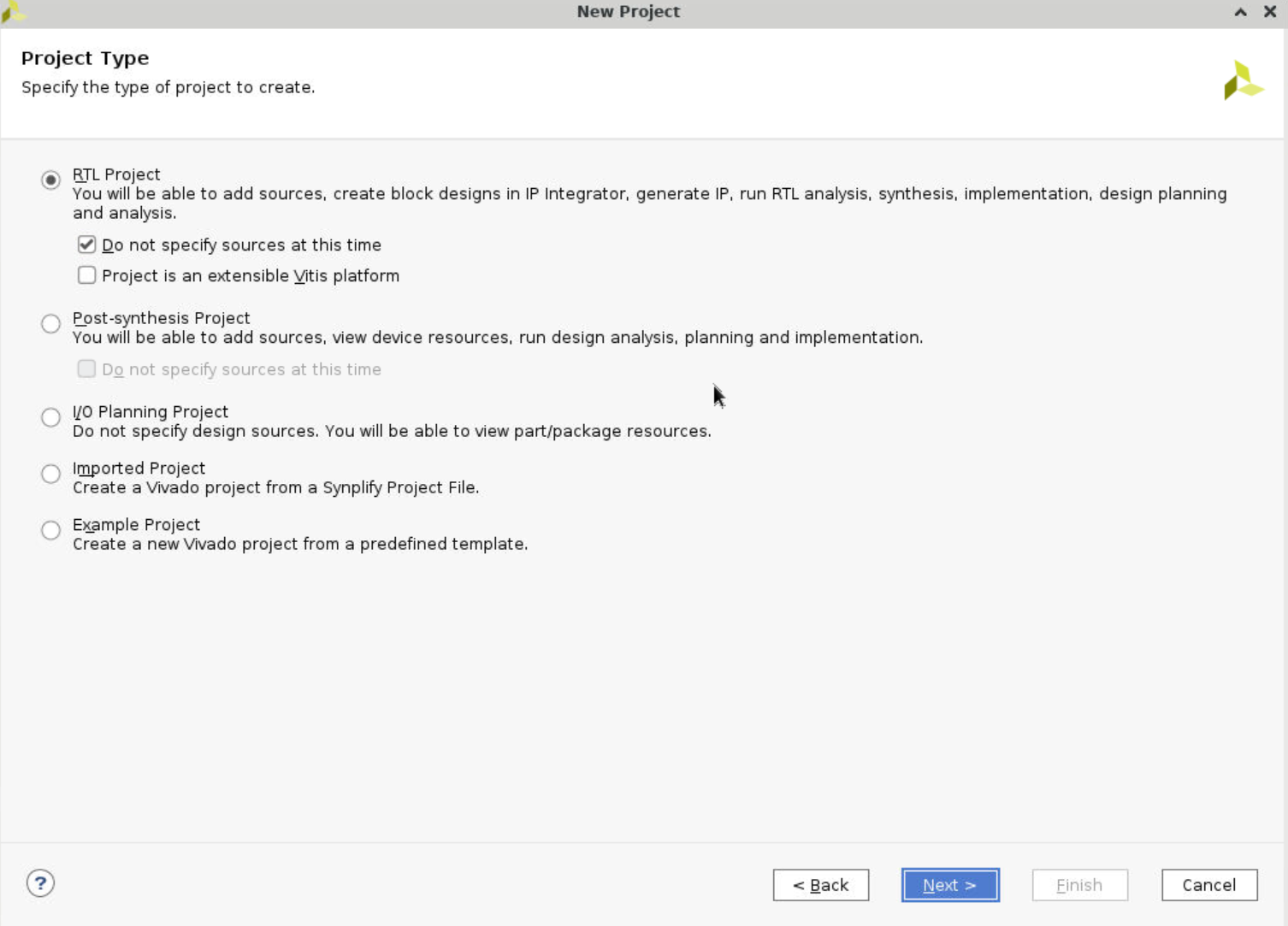
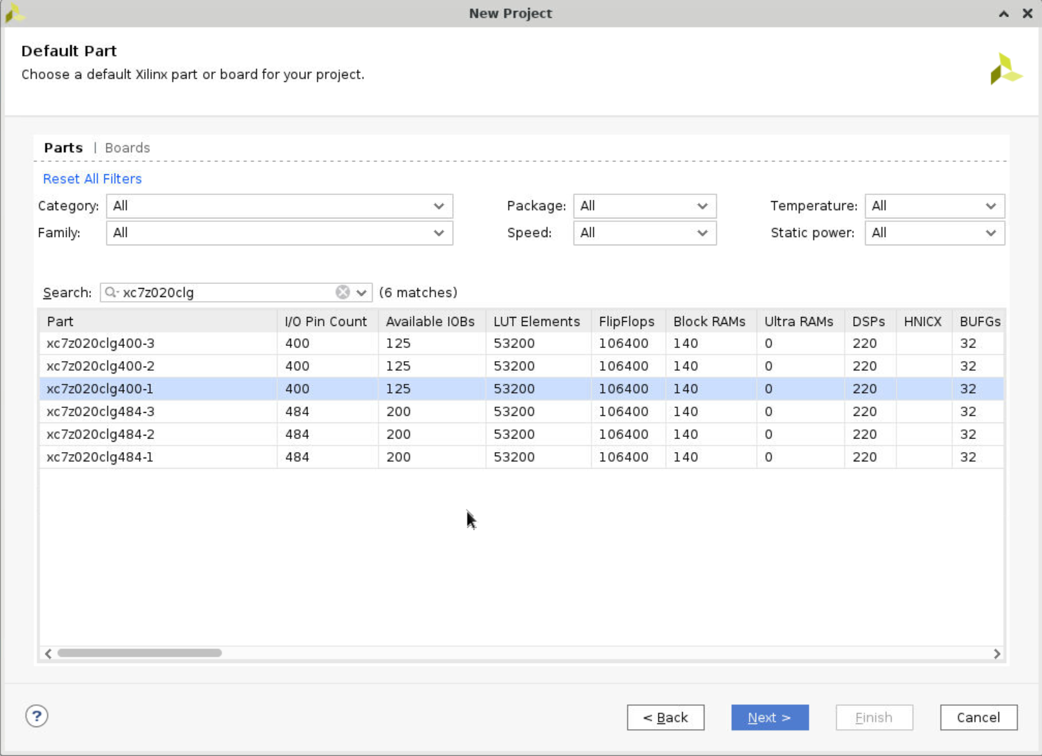
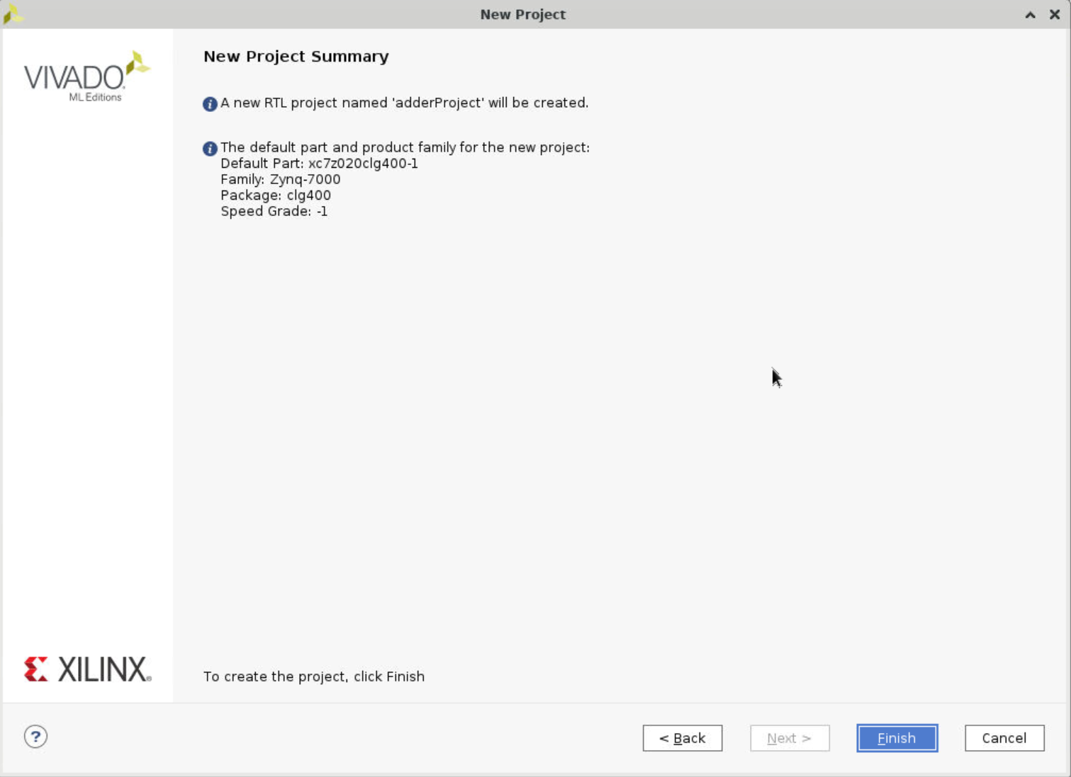
Create a new project, name it as adderProject. Make sure you select the same board you’re using. If you cannot find it, there is an install board icon at top right corner where you can install your own board.
Step 4
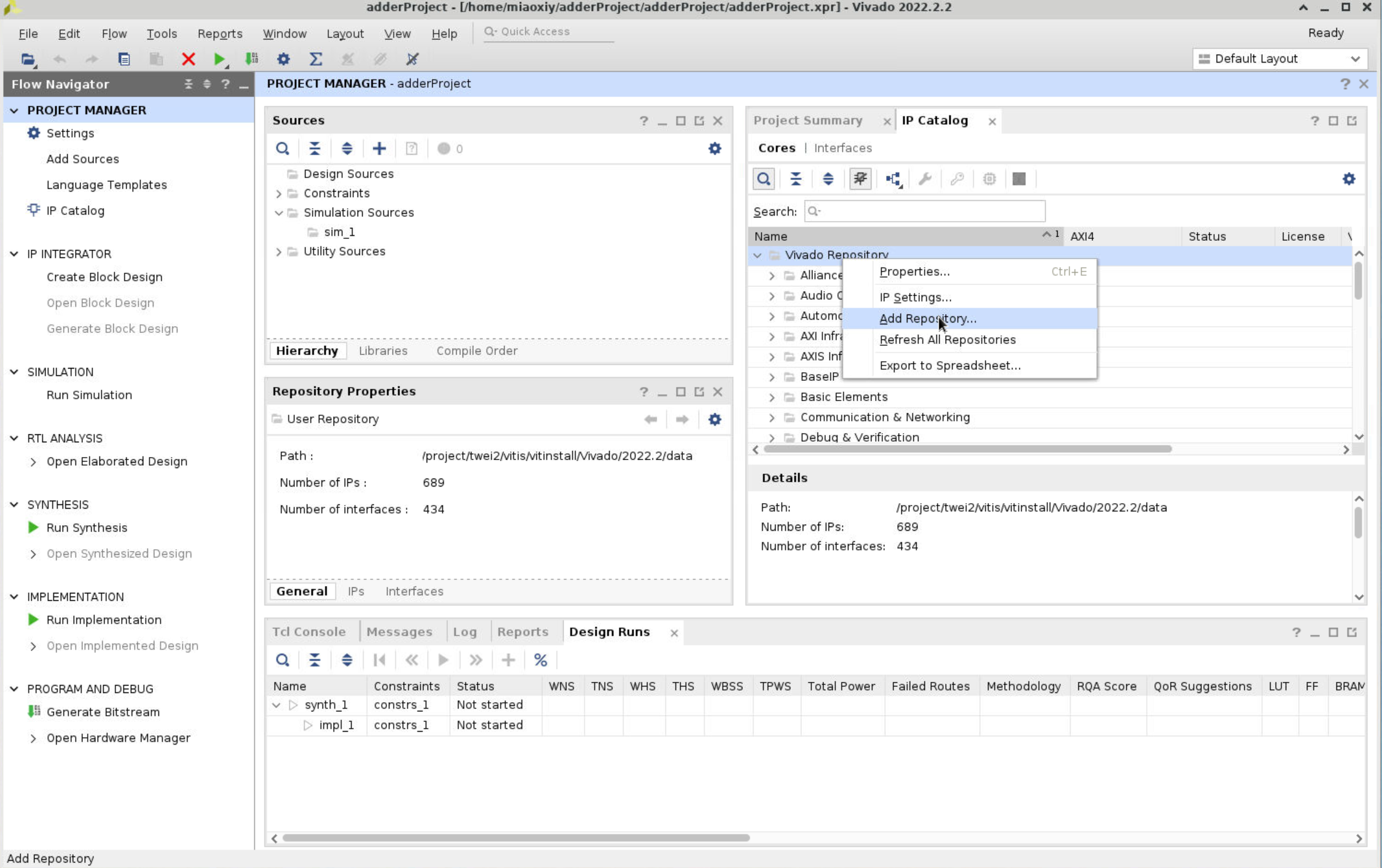
Add our adder IP core to the Vivado. Click IP Catalog at the left column, right click the Vivado Repository, and select Add Repository.
Step 5
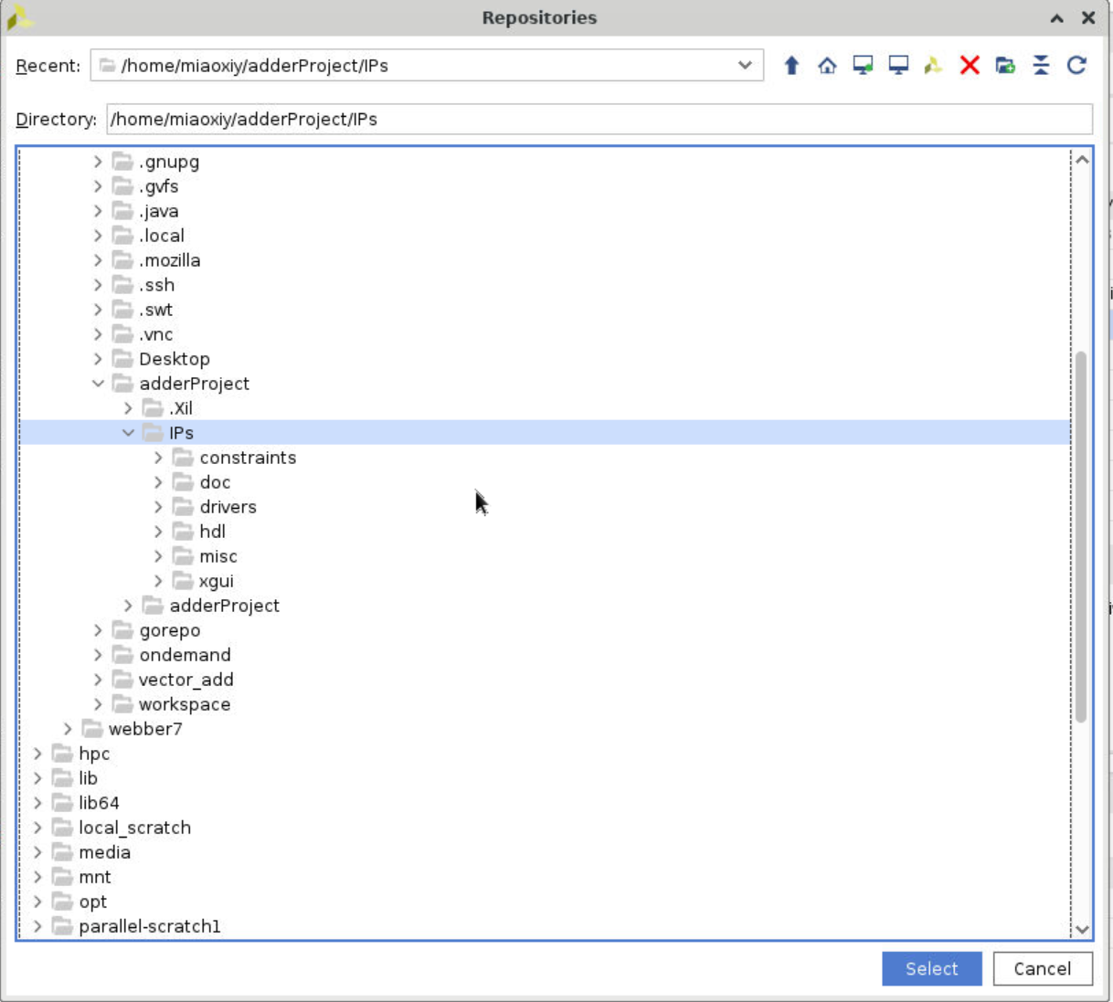
Select the folder that we create before, IPs. Then click select button. The following page should pop up.
Step 6
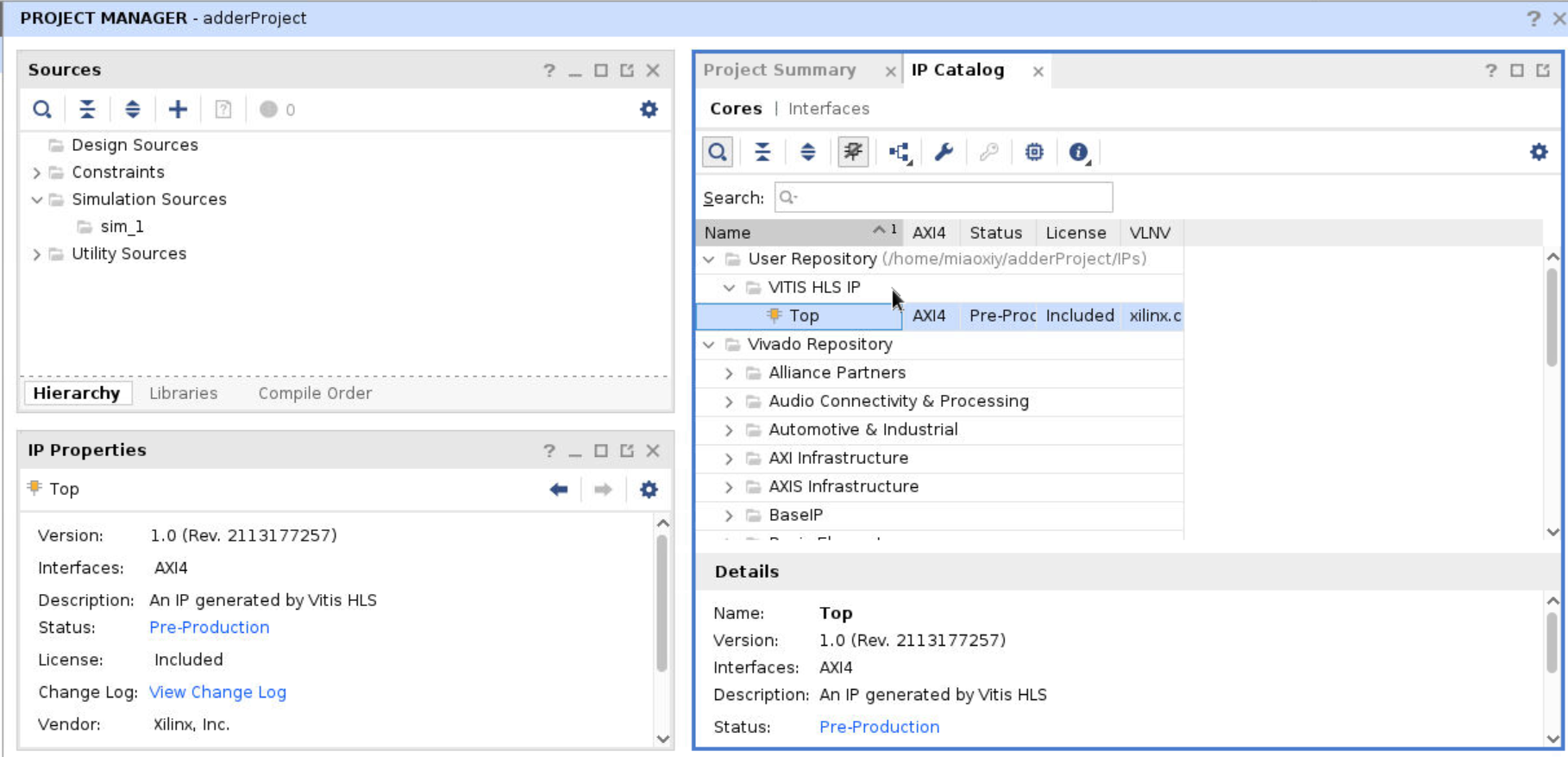
Expand the User Repository, you will see the top IP with an orange icon, there no issue for now. If the icon is grey, re-check whether the same board was chosen as in Vitis.
Step 7
Now we build the block diagram. Click the Create Block Design at the left column. Click the + icon at the upper side of the diagram. Type hls for finding the add function ip. Type zynq to find the embedded controller.
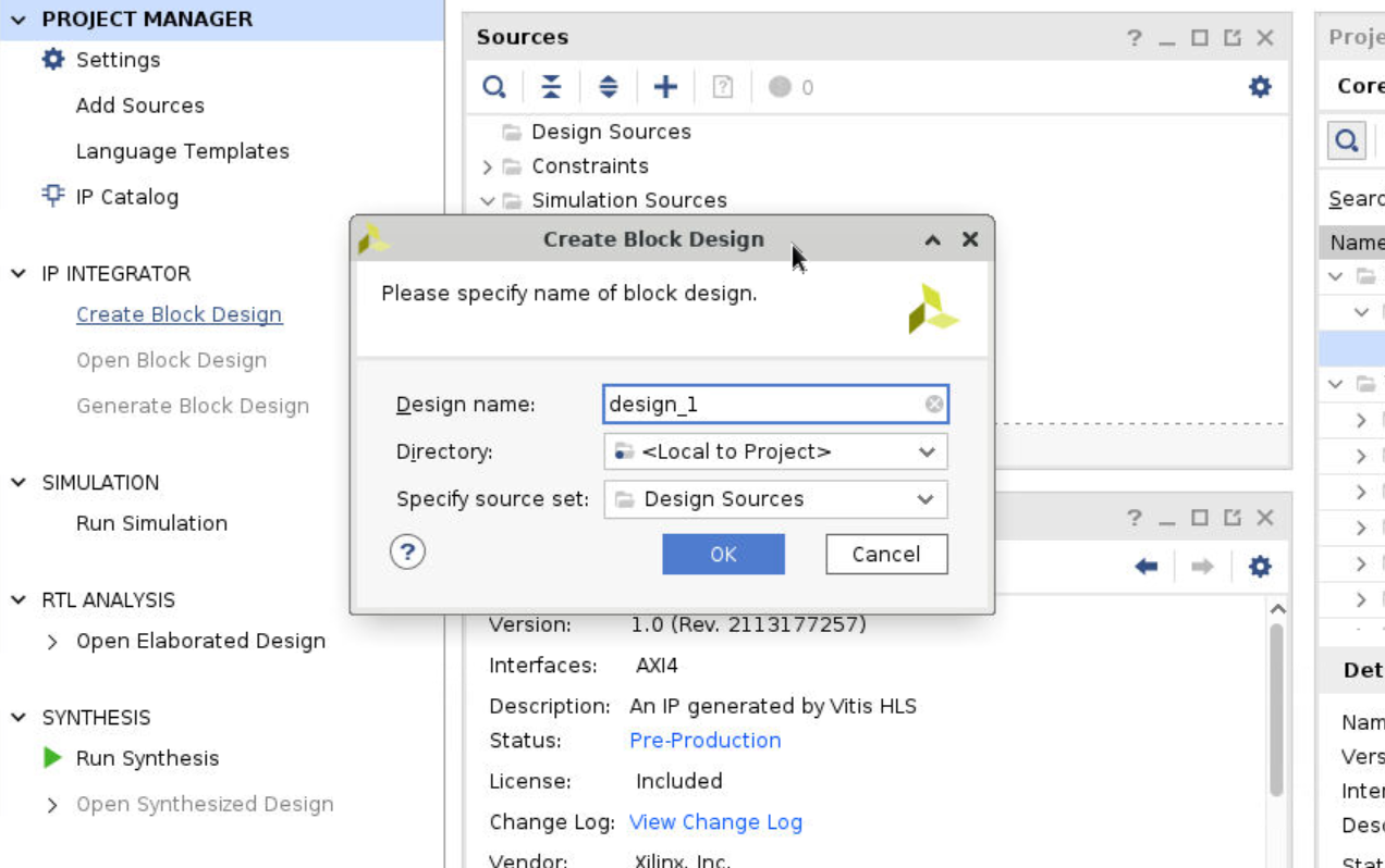
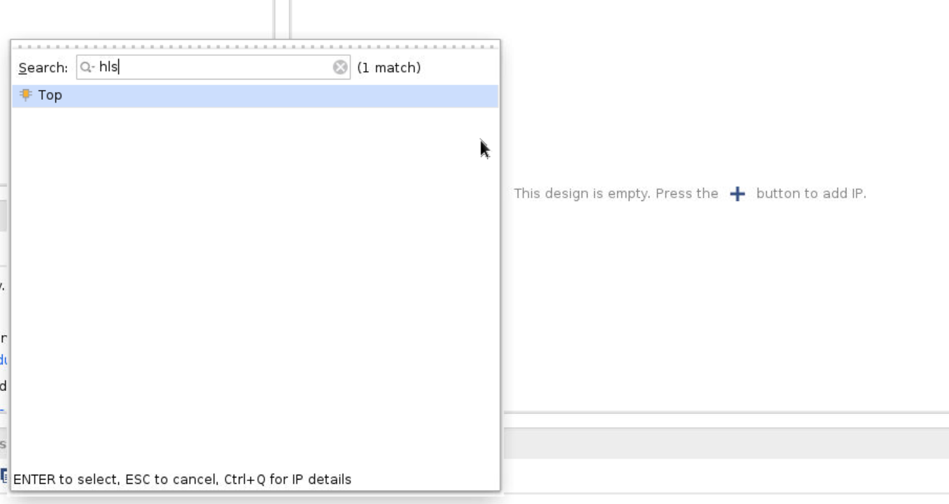
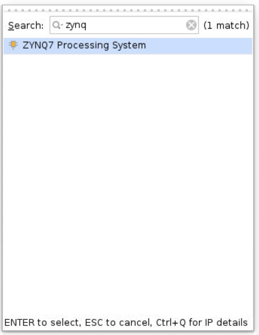
Step 8
Since we specified two inputs and one output in our C code in different “bundles”, we need to initialise 3 AXI buses on the FPGA. To do so, double click the ZYNQ icon on the block diagram. Select PS-PL Configuration. Then, select the S AXI HP0 Interface to S AXI HP2 Interface under HP Slave AXI Interface by checking their boxes.
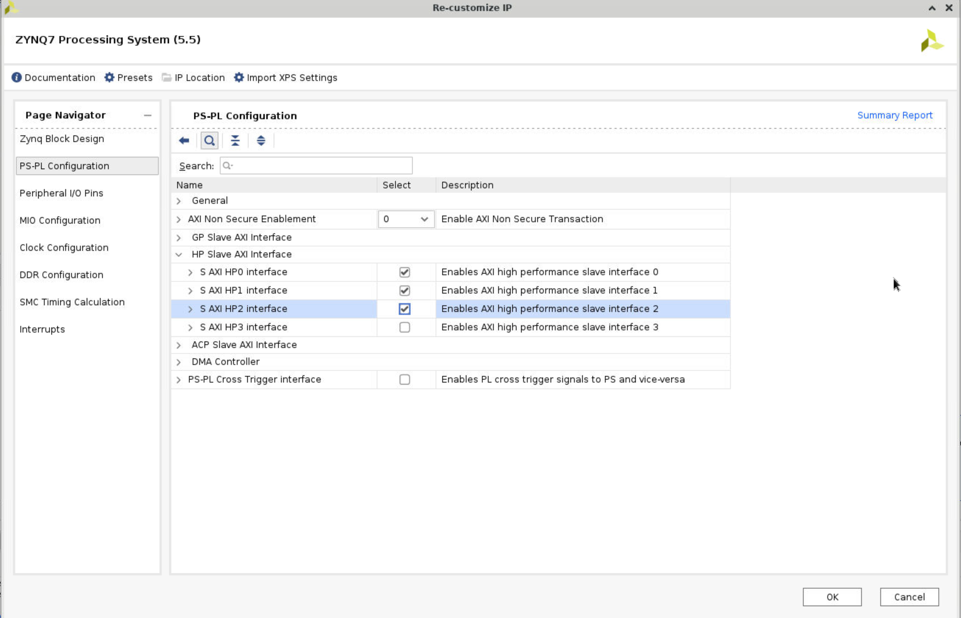
Step 9
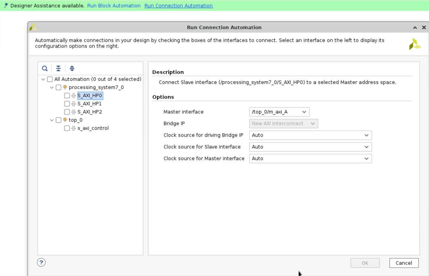
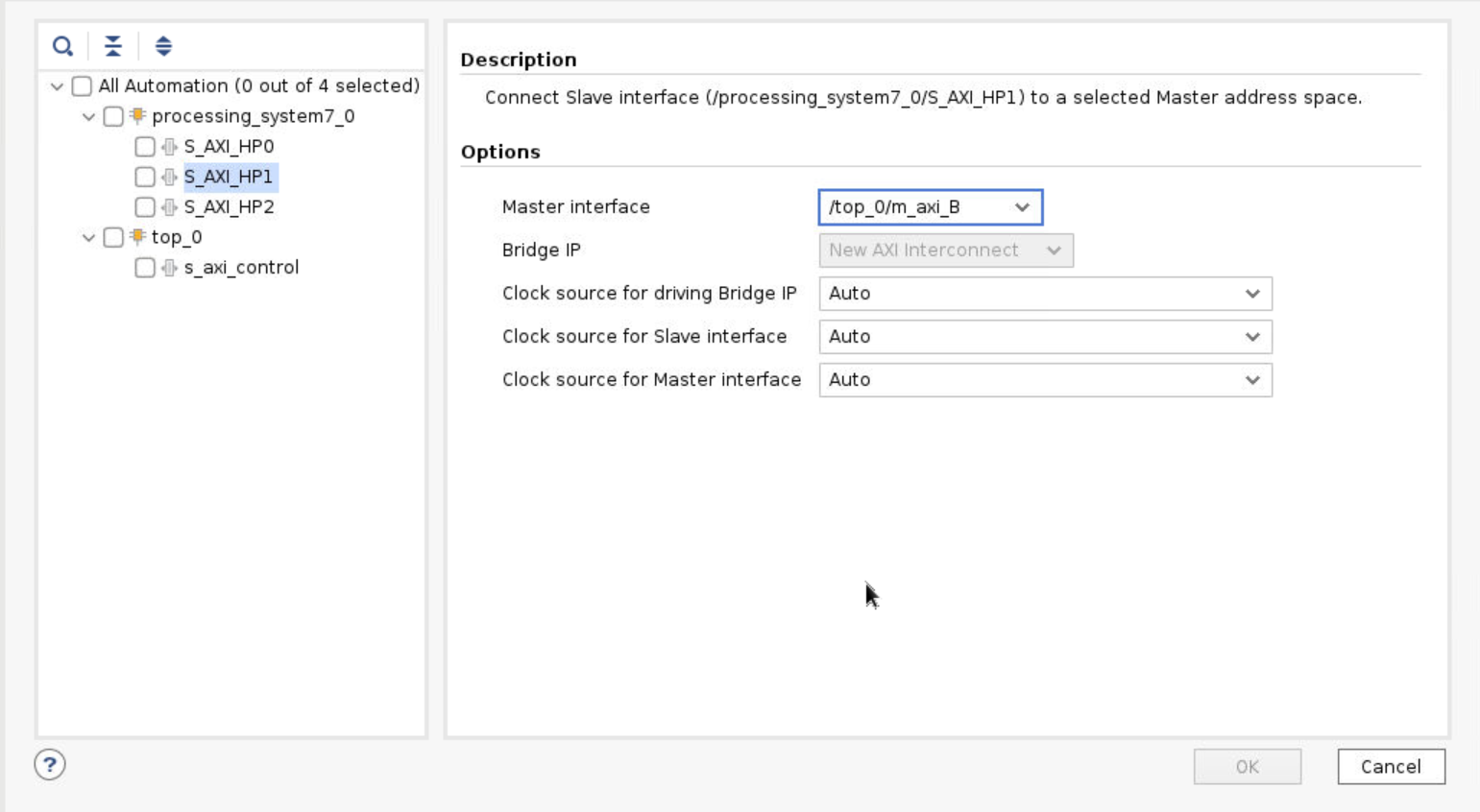
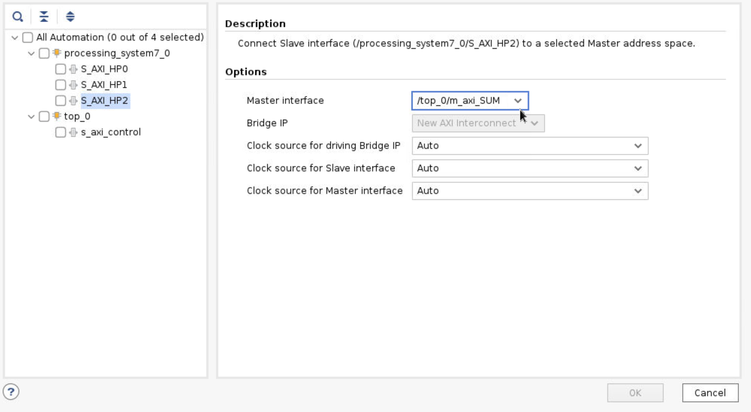
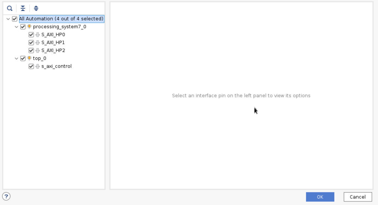
Go back to the Block Diagram and click Run Connection Automation. You need to manually map the HLS ports to the three AXI HP buses in the IP. Then select the All Automation at the left column. Click OK to start connection automation.
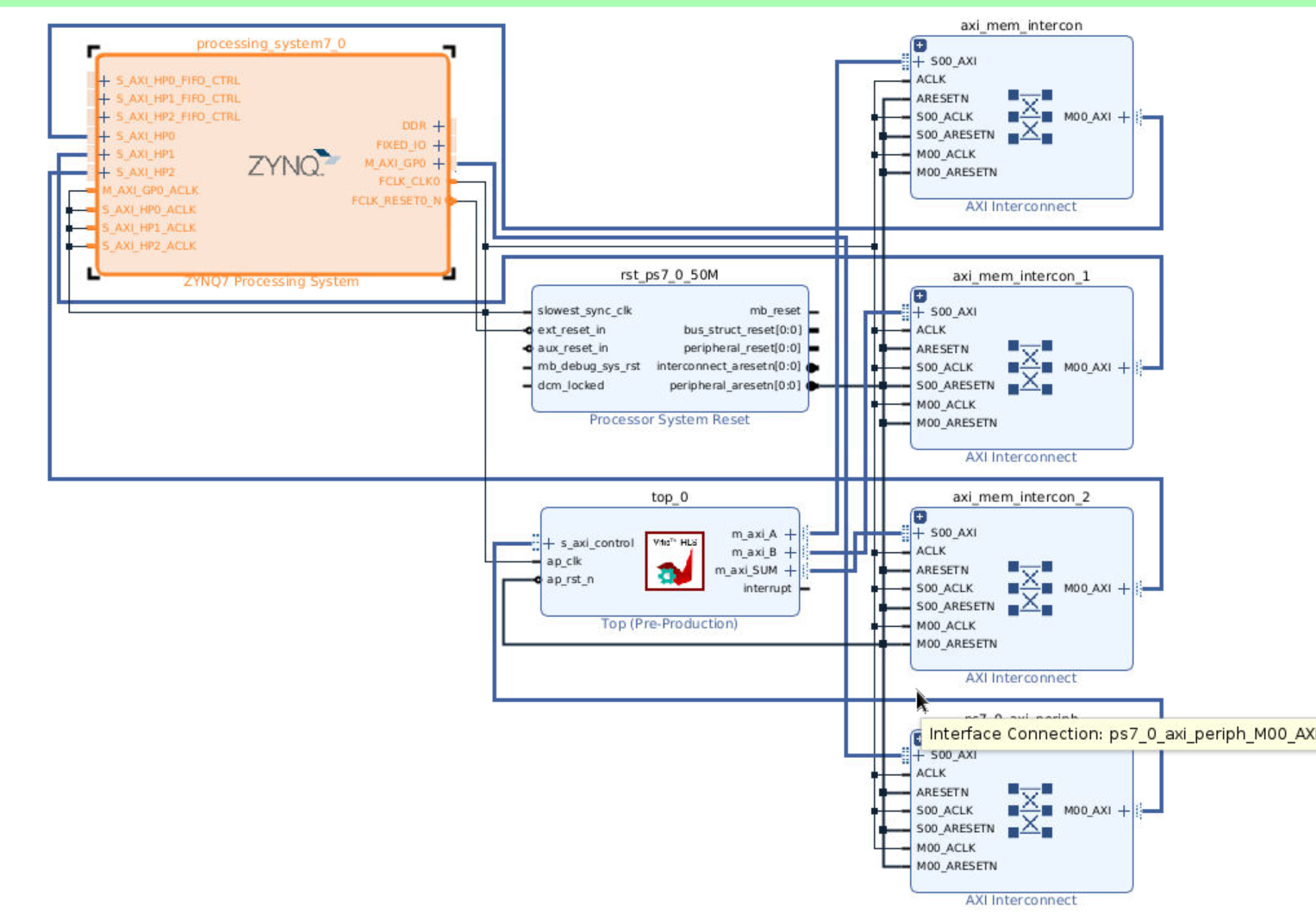
Step 10
To check the correctness, click the validation on the upper page.
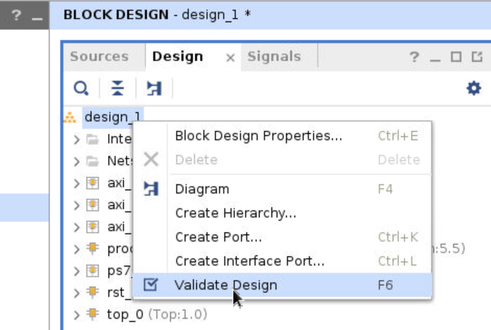
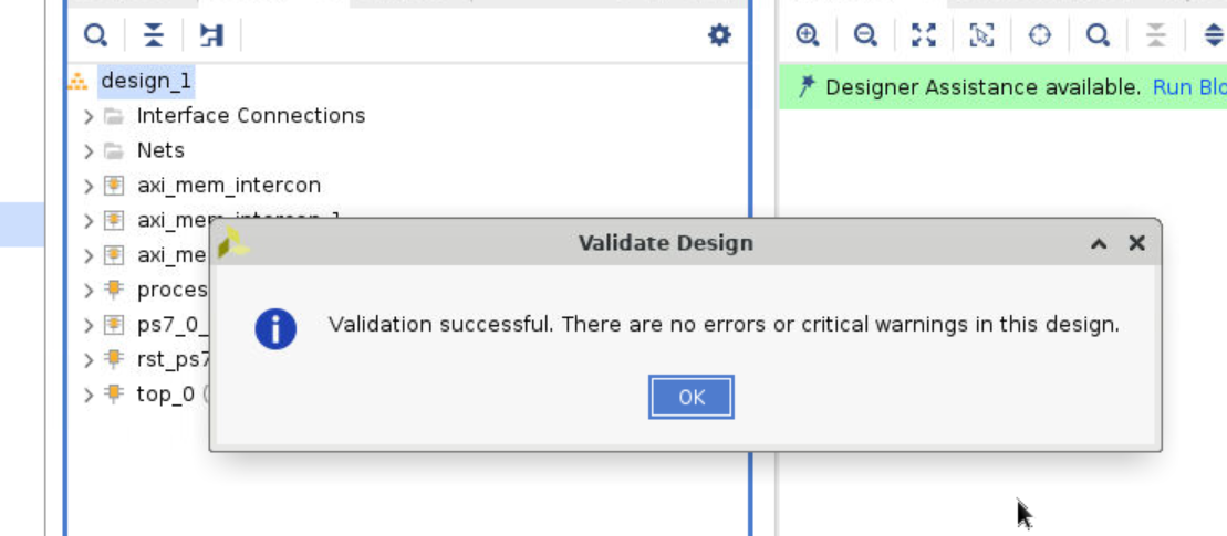
Step 11
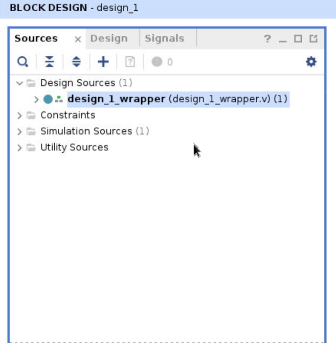
The next step is to create a wrapper for the Block Design. Find the block diagram file under the design sources. Right click the design file (whatever you name it) and select Create HDL Wrapper. Choose Let Vivado manage wrapper and auto-update option. Click OK to start.
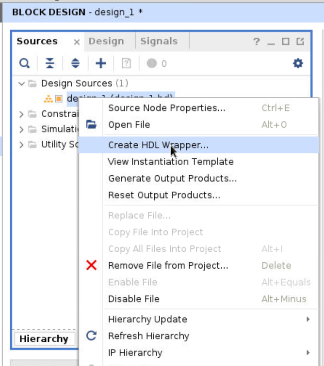
Step 12
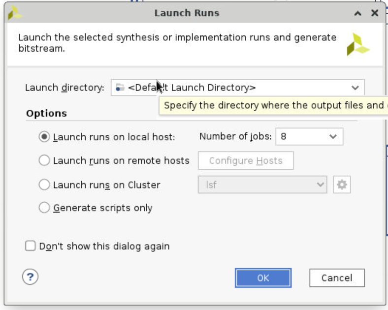
Finally, click Generate Bitstream under PROGRAM AND DEBUG division (at the lower left of the entire page). Use the default settings (for our simple example) and start to run.

Step 13
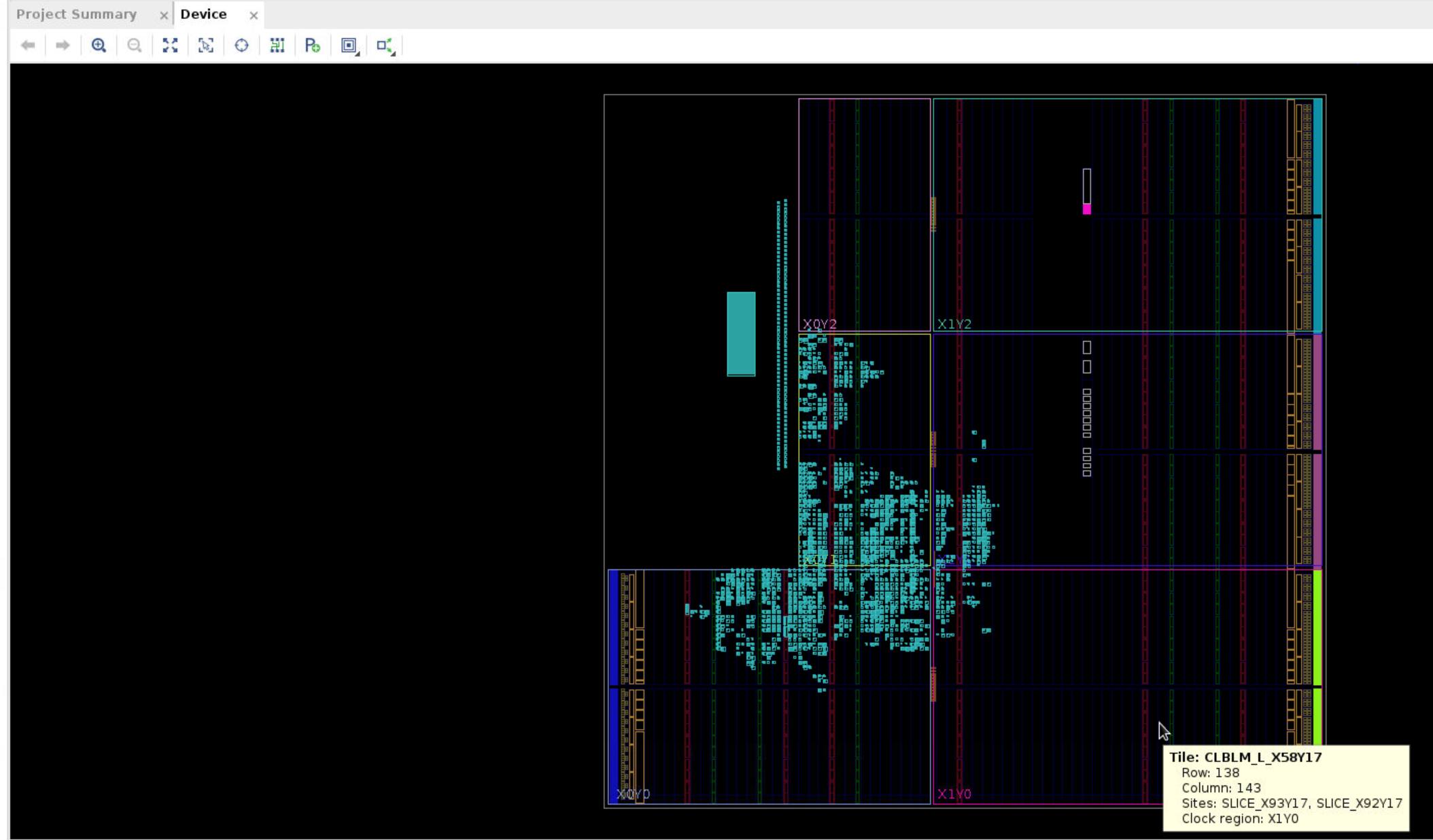
If bitstream generation is successful, you should be able to view the implemented design!
Step 14
After generating the bitstream we need two files for running the vector addition on FPGA: the bitstream with .bit as the extension and the hardware handoff file with .hwh. You can find the .bit file under adderProject/adderProject.runs/impl_1. The .hwh file is under the directory adderProject/adderProject.gen/sources_1/bd/design_1/hw_handoff.
Step 15
You can copy/paste these two files to a flash drive and put them on your own laptop for the next step. Note that these two files must have the same name except for the extension.